SKEDSOFT
Digital to Analog Conversion
The function of a digital to analog converter is to convert a sequence of digital words stored in a data register (called DAC register), typically in the straight binary form, into an analog signal.
The data in the DAC registermay be arriving from a data bus of a computer. Each binary digit (bit) of information in the register may bepresent as a state of a burstable (two-stage) logic device, which can generate a voltage pulse or a voltage level torepresent that bit. For example, the “off state” of a beatable logic element or “absence” of a voltage pulse or“low level” of a voltage signal or “no change” in a voltage level can represent binary 0.
Conversely, the “onstate” of a bitable device or “presence” of a voltage pulse or “high level” of a voltage signal or “change” in avoltage level will represent binary 1.
The combination of these bits forming the digital word in the DACregister will correspond to some numerical value for the analog output signal.
Then, the purpose of the DAC isto generate an output voltage (signal level) that has this numerical value, and maintain the value until the nextdigital word is converted into the analog form. Since a voltage output cannot be arbitrarily large or small forpractical reasons, some form of scaling would have to be employed in the DAC process.
This scale will dependon the reference voltage uref used in the particular DAC circuit.
A typical DAC unit is an active circuit in the integrated circuit form and may consist of a data register (digital circuits), solid-state switching circuits, resistors, and operational amplifiers powered by an external power supply, which can provide the reference voltage for the DAC.
The reference voltage will determine the maximum value of the output (fullscale voltage). As noted before, the integrated circuit (IC) chip that represents the DAC is usually one of many components mounted on a printed circuit (PC) board, which is the input/output (I/O) board (or, I/O card; or, interface board; or, data acquisition and control board).
This board is plugged into a slot of the data acquisition and control PC.
There are many types and forms of DAC circuits. The form will depend mainly on the manufacturer, and requirements of the user or of the particular application.
Most types of DAC are variations of two basic types: the weighted type (or summer type or adder type) and the ladder type.The latter type of DAC is more desirable even though the former type could be somewhat simpler and less expensive.
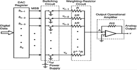
Weighted Resistor DAC
A schematic representation of a weighted-resistor DAC (or summer DAC or adder DAC) Note that this is a general n-bit DAC and n is the number of bits in the output register.
The binary word in the register is
w=[bn-1bn-1bn-3…b1b0]
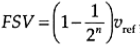
in which bi is the bit in the ith position and it can take the value 0 or 1 depending on the value of the digital output. The decimal value of this binary word is given by
D=2n-1bn-1 2n-2bn-2 ··· 20b0
 Note that the least significant bit (LSB) is b0 and the most significant bit (MSB) is bn-1.
The analog output voltage u of the DAC has to be proportional to D. Each bit bi in the digital word w will activate a solid-state microswitch in the switching circuit, typically by sending a switching voltage pulse.
If bi=1 the circuit lead will be connected to the -urea supply providing an input voltage ui=-urea to the corresponding weighting resistor 2n-i-1R. If, on the other hand bi=0, then the circuit lead will be connected to ground, thereby providing an input voltage ui=0 to the same resistor.