SKEDSOFT
Dual Slope ADC:
This analog to digital converter uses an RC integrating circuit. Hence, it is also known as an integrating ADC. This ADC is simple and inexpensive. In particular, an internal DAC is not utilized and hence, DAC errors as mentioned previously will not enter the ADC output.
Furthermore, the parameters R and C in the integrating circuit do not enter the ADC output. As a result, the device is self-compensating with regard to circuitparameter variations due to temperature, aging, etc.
A shortcoming of this ADC is its slow conversion rate because, for accurate results, the signal integration has to proceed for a longer time in comparison to the conversion time for a successive approximation ADC.
Analog-to-digital conversion in a dual slope ADC is based on timing (i.e., counting the number of clock pulsesm during) a capacitor-charging process.
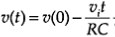
The principle of operation can be explained with reference to the integrating circuit. Note that ui is a constant input voltage to the circuit and u is the output voltage.
Since the “ ” lead of the op-amp is grounded, the “-” lead (and node A) also will have zero voltage. Also, the currents through the op-amp leads are negligible.
Hence, the current balance at node A gives

A schematic diagram for a dual slope ADC.
Initially, the capacitor C in the integrating circuit is discharged (zero voltage).
Then, the analog signal us is supplied to the switching element and held constant by the sample and hold circuit (S/H).
Simultaneously, a “conversion starts” (CS) control signal is sent to the control logic unit.
This will clear the timer and the output register (i.e., all bits are set to zero) and will send a pulse to the switching element to connect the input us to the integrating circuit.
Also, a signal is sent to the timer to initiate timing (counting). The capacitor C will begin to charge.
