SKEDSOFT
Introduction:
Early strain gages were fine metal filaments. Modern strain gages are manufactured primarily as metallic foil (e. g., using the copper-nickel alloy known as constantan) or semiconductor elements (e.g., silicon with trace impurity boron).
They are manufactured by first forming a thin film (foil) of metal or a single crystal of semiconductor material and then cutting it into a suitable grid pattern, either mechanically or by using photo etching (opto-chemical) techniques. This process is much more economical and is more precise than making strain gages with metal filaments. The strain gage element is formed on a backing film of electrically insulated material (e.g., polymide plastic).
This element is cemented or bonded using epoxy, onto the member whose strain is to be measured. Alternatively, a thin film of insulating ceramic substrate is melted onto the measurement surface, on which the strain gage is mounted directly. The direction of sensitivity is the major direction of elongation of the strain gage element.
To measure strains in more than one direction, multiple strain gages (e.g., various rosette configurations) are available as single units.
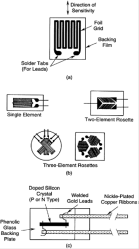
 These units have more than one direction of sensitivity Principal strains in a given plane (the surface of the object on which the strain gage is mounted) can be determined by using these multiple strain gage units. Typical foil-type gages are shown in Figure (b), and a semiconductor strain gage is shown in Figure (c).
A direct way to obtain strain gage measurement is to apply a constant dc voltage across a series-connected pair of strain gage element (of resistance R) and a suitable resistor Rc, and to measure the output voltage uo across the strain gage under open-circuit conditions (using a voltmeter with high input impedance). It is known as a potentiometer circuit or ballast circuit.
This arrangement has several weaknesses.
Any ambient temperature variation will directly introduce some error because of associated change in the strain gage resistance and the resistance of the connecting circuitry Also, measurement accuracy will be affected by possible variations in the supply voltage uref.
 Furthermore, the electrical loading error will be significant unless the load impedance is very high. Perhaps the most serious disadvantage of this circuit is that the change in the signal due to strain is usually a very small percentage of the total signal level in the circuit output. This problem can be reduced to some extent by decreasing uo, which may be accomplished by increasing the resistance Rc.
This, however, reduces the sensitivity of the circuit. Any changes in the strain gage resistance due to ambient changes will directly enter the strain gage reading unless R and Rc have identical coefficients with respect to ambient changes.