SKEDSOFT
Introduction: Boolean algebra is used to model the circuitry of electronic devices. Each input and each output of such a device can be thought of as a member of the set {0, 1}.A computer, or other electronic device, is made up of a number of circuits. Each circuit can be designed using the rules of Boolean algebra that were studied in Boolean algebra. The basic elements of circuits
are called gates. Each type of gate implements a Boolean operation. In this section we define several types of gates. Using these gates, we will apply the rules of Boolean algebra to design circuits that perform a variety of tasks. The circuits that we will study in this chapter give output that depends only on the input, and not on the current state of the circuit. In other words, these circuits have no memory capabilities. Such circuits are called combinational circuits or gating networks.
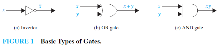
We will construct combinational circuits using three types of elements. The first is an inverter, which accepts the value of one Boolean variable as input and produces the complement of this value as its output. The symbol used for an inverter is shown in Figure 1(a). The input to the inverter is shown on the left side entering the element, and the output is shown on the right side leaving the element.
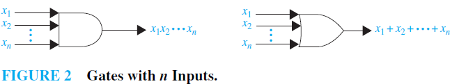
The next type of element we will use is the OR gate. The inputs to this gate are the values of two or more Boolean variables. The output is the Boolean sum of their values. The symbol used for an OR gate is shown in Figure 1(b). The inputs to the OR gate are shown on the left side entering the element, and the output is shown on the right side leaving the element. The third type of element we will use is theAND gate. The inputs to this gate are the values of two or more Boolean variables. The output is the Boolean product of their values. The symbol used for anAND gate is shown in Figure 1(c). The inputs to theAND gate are shown on the left side entering the element, and the output is shown on the right side leaving the element. We will permit multiple inputs to AND and OR gates. The inputs to each of these gates are shown on the left side entering the element, and the output is shown on the right side. Examples of AND and OR gates with n inputs are shown in Figure 2.
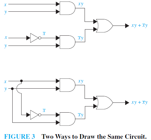
Combinations of Gates: Combinational circuits can be constructed using a combination of inverters, OR gates, andAND gates. When combinations of circuits are formed, some gates may share inputs. This is shown in one of two ways in depictions of circuits. One method is to use branchings that indicate all the gates that use a given input. The other method is to indicate this input separately for each gate. Figure 3 illustrates the two ways of showing gates with the same input values. Note also that output from a gate may be used as input by one or more other elements, as shown in Figure 3. Both drawings in Figure 3 depict the circuit that produces the output 
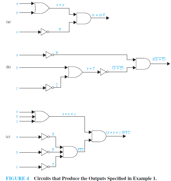
EXAMPLE 1 Construct circuits that produce the following outputs: 
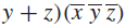
Solution: Circuits that produce these outputs are shown in Figure 4.