SKEDSOFT
Successive Approximation ADC
This type of analog to digital converter is very fast, and is suitable for high-speed applications. The speed of conversion depends on the number of bits in the output register of ADC but is virtually independent of the nature of the analog input signal.
A schematic diagram for a successive approximation ADC Note that a DAC is an integral component of this ADC. The sampled analog signal (from a sample and hold circuit) is applied to a comparator (typically a differential amplifier). Simultaneously, a “start conversion” (SC) control pulse is sent into the control logic unit by the external device.
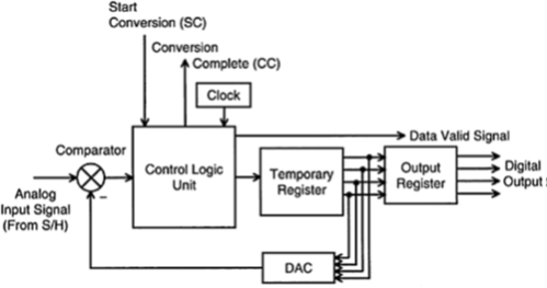
ADC until a “conversion complete” (CC) pulse is sent out by the control logic unit. Initially, the registers are cleared so that they contain all zero bits. Now, the ADC is ready for its first conversion approximation. The first approximation begins with a clock pulse.
Then, the control logic unit will set the most significant bit (MSB) of the temporary register (DAC control register) to 1, all the remaining bits in that register being zero.
This digital word in the temporary register is supplied to the DAC. Note that the analog output of the DAC is now equal to half the full-scale value.
This analog signal is subtracted from the analog input by the comparator. If the output of the comparator is positive, the control logic unit will keep the MSB of the temporary register at binary 1 and will proceed to the next approximation. If the comparator output is negative, the control logic unit will change the MSB to binary 0 before proceeding to the next approximation.
The second approximation will start at another clock pulse. This approximation will consider the second most significant bit of the temporary register.
As before, this bit is set to 1 and the comparison is made. If the comparator output is positive, this bit is left at value 1 and the third most significant bit is considered.
If the comparator output is negative, the bit value will be changed to 0 before proceeding to the third most significant bit.
Analog to Digital Conversion
Analog signals, which are continuously defined with respect to time, have to be sampled at discrete time points and the sample values have to be represented in the digital form (according to a suitable code) to be read into a digital system such as a microcomputer.
An ADC is used to accomplish this. For example, since response measurements of a mechatronic systems are usually available as analog signals, these signals have to be converted into the digital form before passing on to a digital computer for analysis and possibly generating a control command. Hence, the computer interface for the measurement channels should contain one or more ADCs.
DACs and ADCs are usually situated on the same digital interface board. The analog to digital conversion process is more complex and time consuming than the digital to analog conversion process. Furthermore, many types of ADCs use DACs to accomplish the analog to digital conversation. Hence, ADCs are usually more costly, and their conversion rate is usually slower in comparison to DACs.
Several types of analog to digital converters are commercially available. The principle of operation may vary depending on the type. A few commonly known types are discussed here.
